Electronics
AI PCB design for beginners: a one-button desk mute board
AI PCB design for beginners: draft a low-voltage USB mute button, keep to JLCPCB Basic Parts, order a small board, and print a case.
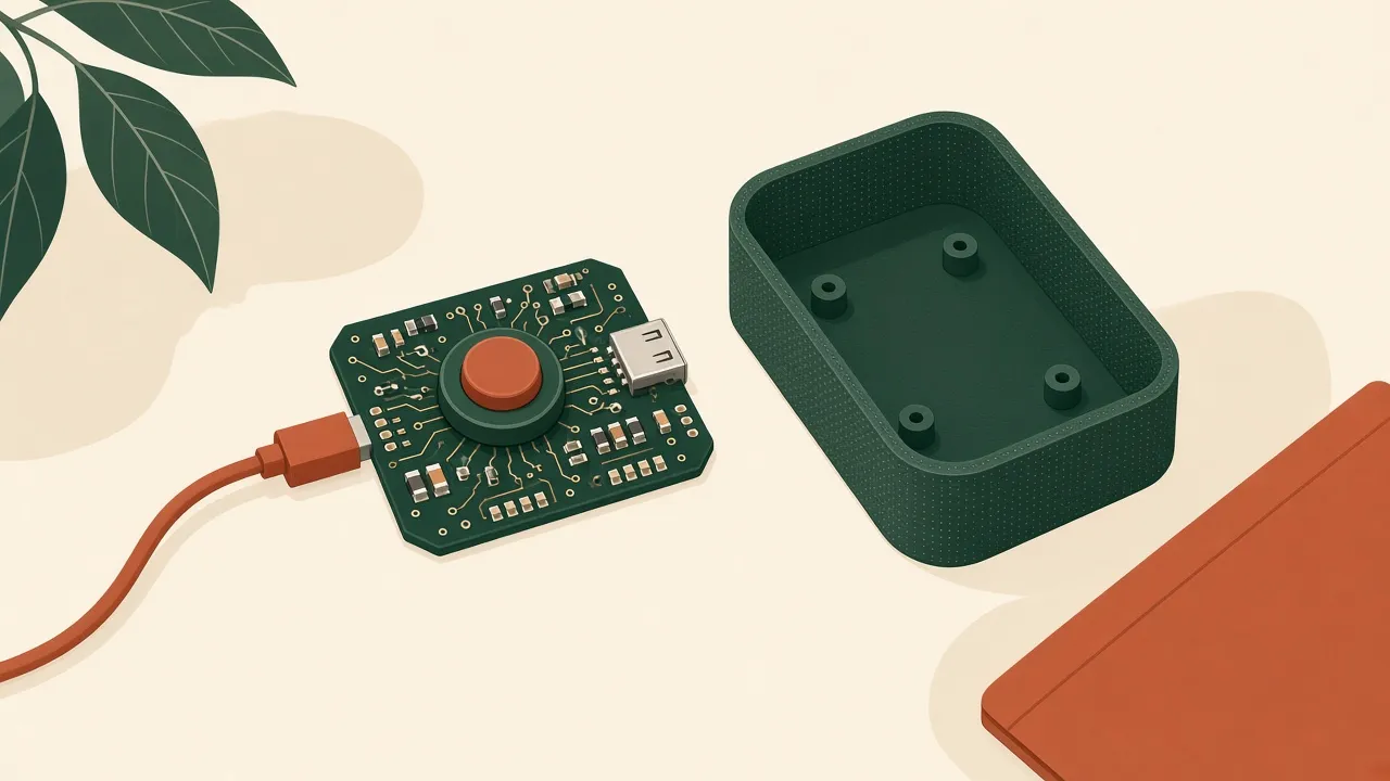
Call software already has a mute key. People still want a button they can hit without finding the window. A one-button board is a good first vibe-manufactured PCB because the circuit is allowed to stay boring: USB power, a switch, and a microcontroller board you did not have to invent.
The loop is the one in what vibe manufacturing is, with Gerbers where a bracket would have had a DXF.
The problem
You want a physical control that sends a single, predictable action to the computer. Mute is the usual one. The failure mode you are designing against is a board that tries to be a product: a battery, a radio, a display, a wall plug.
The honest version:
- A small USB-capable module you can program yourself, or already know how to program.
- A custom board that is mostly a button, a connector, and a mounting pattern for that module. Or no custom board at all for the first week, just the module and a printed case, with the PCB as the second pass.
- A case printed or laser-cut to fit the button you bought, not a button the model imagined.
You are not building a mains controller, a conference system, or a certified USB device for sale. If you later sell it, product rules are a separate project. This note is a desk object for you.
Workflow
1. Measure
Buy the button and the module first. Then measure those, instead of prompting a fantasy footprint.
- The button’s footprint from its datasheet: pad spacing, height, and the actuator diameter. The datasheet wins over a caliper if they disagree, but check the part in your hand against the drawing.
- The module’s mounting holes and the USB connector’s overhang. The plug has to clear the case.
- The desk space you will actually give it. A 40 mm square is easier to finish than a console.
Write millimeters. Save the datasheet PDF next to the notes. A dog-door panel adapts a lock you bought. This board adapts a module you bought. Same idea, lower voltage.
2. Prompt for a PCB
Ask a tool that can emit KiCad, or a PCB assistant you can export from, for a carrier. Keep the electrical ask tiny.
Design a 40 mm by 40 mm, 2-layer PCB.
It carries a purchased USB microcontroller module using the header
footprint I will attach, plus one momentary button and a pull resistor
recommended by that module's examples.
USB power only. No battery, no mains, no boost converter.
Include mounting holes 3.2 mm, 4 mm from each corner.
Export a KiCad project or Gerber and drill files.
Run a design-rule check and list the track width and clearance you used.
Attach the real footprint. If the tool will not export Gerbers or a project file, it has not designed a board. A green rendering is a picture.
3. Prototype
Before the fab order, wire the button to the module on a breadboard or with short leads and confirm the computer sees the action you think you programmed. Order boards only after the firmware gesture works. A panel of beautiful PCBs will not debug a mute shortcut you never tested.
Print or cardboard the case around the real module and the real button. Check that a USB cable seats. The display stands article is the same cardboard-before-acrylic lesson, applied to a shell.
4. Review
Open the Gerbers in a viewer. Look at the board outline, the drill file, and the button pads. Compare copper-to-edge clearance and minimum drill with the fab’s current rules. JLCPCB and PCBWay are examples of fabs that publish those rules. They change. The page on their site is the rule, not this article.
Confirm there is no mains symbol, no battery holder, and no copper you do not understand. Delete decorative copper that gets close to the USB connector. If a net is named “mains,” scrap the project and start over.
5. Send it to a fabricator
Order a small quantity of the 2-layer board. Assembly of one button is something you can solder. If you ask the fab to assemble, you are now also producing a bill of materials with exact part numbers. That is worth doing, and it is a longer job than soldering one switch.
Print the case at home or through a print farm after the board is in your hand, not from the rendering. Connectors grow a millimeter between the render and the parcel.
Program the action you tested. Label the button. A mute key that sometimes opens a menu is worse than no button.
Tools and services
- The module and the button, plus their datasheets.
- KiCad, or another PCB tool you can open. An AI assistant that emits a KiCad project or Gerbers is a draft, not a release.
- A Gerber viewer and the fab’s design-rule page.
- A fab such as JLCPCB or PCBWay for the boards. Read the quote.
- A printer or a laser shop for the case. A sheet shop is usually overkill for a 40 mm lid, and a local printer is not.
Cost and time
Estimate, not a quote. A handful of small 2-layer boards is often a modest line item, and shipping plus the module plus the button often costs as much as the boards. A planning range around $30–$90 before shipping is a way to decide if the button is worth a weekend. Board size, color, thickness, and whether you pay for assembly all move the quote. Read the quote. This is not a price from any fab.
Estimate, not a schedule. Schematic, cardboard case, and a firmware test can be a weekend if the module is one you know. The fab’s build time and the ship time are on their page and in the checkout, and they are not a number this site should freeze in a paragraph. A second board revision is normal if the footprint was wrong. Order the small quantity first for that reason.
Pitfalls
- A from-scratch USB chip because it sounded more impressive than a module.
- Any connection to wall power.
- A battery stuffed in the case without the cell maker’s protection circuit. Skip the battery. USB is right there.
- Ordering from a rendering. Export the Gerbers and open them.
- Ignoring the fab’s minimum drill or solder-mask rules, then being surprised by a note in the order.
- A case designed around the 3D render of the button instead of the button you bought.
- Firmware that fires the wrong key in the wrong app. Test it on a call you can afford to interrupt, or before the call.
- Cloning a commercial mute button’s enclosure. Make a box that fits your module.
Beyond the mute button: AI PCB design for beginners
Sources for this section: Business Insider’s vibe manufacturing feature (November 1, 2026) and public posts on X, linked inline. Short quotes only. Nobody named here has reviewed or endorsed this article.
Once the one-button board works, the same loop scales to more ambitious gadgets. Some public examples:
- A kids’ story toy, ten units. Business Insider describes an IT worker, Arthur Prince, who built a storytelling toy for his daughter with GPT-6 Astra and Claude, had one model critique the other’s design, and ordered ten units from JLCPCB for about €500 (reported figure).
- A desk companion enclosure. @tylermart shared on X an AI-designed mini-mech enclosure for an M5Stack AtomS3R module, printed on a Bambu Lab P1S.
- A solder-paste stencil. @allenmeng posted that Codex modelled a PLA 3D-printed solder-paste stencil from PCB files, a neat way to use the board files twice.
- Rules for cheaper boards. @0x7c0x80386 shared Claude PCB design rules aimed at sticking to JLCPCB Basic Parts.
A beginner workflow for any small board
- Start from a module. An ESP32 or M5Stack board does the hard radio and power work. Your PCB can be a simple carrier.
- Describe the circuit in plain words: inputs, outputs, supply voltage, connectors, board size.
- Ask the AI to prefer JLCPCB Basic Parts and to list each part with its LCSC number so you can verify stock yourself.
- Get files you can open, such as a KiCad project, and run KiCad’s ERC and DRC yourself.
- Order a few bare boards first. Assembly can wait until the first board powers up.
- Design the case last, from the real board dimensions. See how to make a 3D-printable part with AI.
Common beginner mistakes
- Footprints that do not match the chosen part.
- Missing decoupling capacitors or a wrong regulator pinout.
- A case drafted before the board was final.
- Trusting the render. As one builder told Business Insider about his project, “AI’s good but not perfect.”
Keep every AI-drafted board to USB or battery power. Anything on mains power needs qualified design and certification.
FAQ
Should the board plug into the wall?
No. Keep this project on USB low voltage from the computer. Do not design a mains supply, a lamp dimmer, or anything that leaves the USB connector's voltage.
Can an AI tool emit a finished Gerber I can order blindly?
It can draft a schematic and a layout. You still open the files, run the design-rule check, and compare the result with the fab's current rules. A rendered picture of a green board is not an order.
Why use a module instead of a bare USB chip?
A small USB-capable board you already understand, with one button wired to it, is a finishable project. A from-scratch USB stack is a different project, and a generated one is a good way to order a board that enumerates as nothing.
Is the price range a JLCPCB quote?
No. It is a rough planning estimate for a handful of small boards plus parts and a case. Shipping, board size, and assembly options move it. Read the quote.
Can AI design a PCB?
AI tools can draft schematics, pick parts, and write layout scripts or KiCad files for simple low-voltage boards. Hobbyists have shared boards made this way, but every design still needs a design-rule check and careful review.
What are JLCPCB Basic Parts?
They are components JLCPCB keeps loaded for assembly. Using them can avoid extra setup fees for extended parts. Check JLCPCB's current parts library and fee rules.
Is JLCPCB sponsoring this?
No. JLCPCB is named because it appears in public examples. It has not reviewed or endorsed this article.